| CPC G11C 7/222 (2013.01) [G11C 7/225 (2013.01); G11C 2207/2272 (2013.01)] | 26 Claims |
|
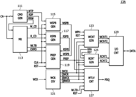
1. A semiconductor device comprising:
a pre-pulse generation circuit configured to generate a pre-pulse, based on a write/read shifting pulse and a write leveling activation signal;
a write/read control signal generation circuit configured to generate a write/read control signal, based on the pre-pulse and a division clock; and
a write leveling control circuit configured to generate detection data including information on a phase difference between a data clock and a system clock, based on the pre-pulse and the division clock,
wherein a pulse width of the pre-pulse is set based on a frequency ratio of the system clock and the data clock when a write/read operation is performed.
|