US 11,741,913 B2
Methods and circuits for diode-based display backplanes and electronic displays
Sean William Muir, Corvallis, OR (US); and Christopher Harold Koch, Corvallis, OR (US)
Assigned to Amorphyx, Incorporated, Corvallis, OR (US)
Appl. No. 17/311,303
Filed by Amorphyx, Incorporated, Corvallis, OR (US)
PCT Filed Dec. 6, 2019, PCT No. PCT/US2019/065089
§ 371(c)(1), (2) Date Jun. 4, 2021,
PCT Pub. No. WO2020/118268, PCT Pub. Date Jun. 11, 2020.
Claims priority of provisional application 62/776,931, filed on Dec. 7, 2018.
Prior Publication US 2022/0028345 A1, Jan. 27, 2022
Int. Cl. G09G 3/34 (2006.01); G09G 3/36 (2006.01)
CPC G09G 3/344 (2013.01) [G09G 3/367 (2013.01); G09G 3/3648 (2013.01); G09G 2300/0417 (2013.01); G09G 2300/0895 (2013.01); G09G 2310/0262 (2013.01)] 17 Claims
OG exemplary drawing
 
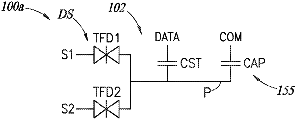
1. A pixel device, comprising:
a first non-linear element coupled between a first selection line and a charging node;
a second non-linear element coupled between a second selection line and the charging node, the first and second non-linear elements include an amorphous metal non-linear resistor;
a charging capacitive element coupled between a data line and the charging node; and
a pixel element coupled between the charging node and a common electrode.