| CPC G09G 3/3275 (2013.01) [G09G 3/325 (2013.01); G09G 3/006 (2013.01); G09G 3/3233 (2013.01); G09G 3/3291 (2013.01); G09G 2310/0297 (2013.01); G09G 2330/08 (2013.01); G09G 2330/12 (2013.01)] | 4 Claims |
|
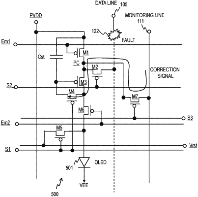
1. A display device comprising:
a pixel circuit on a substrate;
a data line configured to transmit a data signal for the pixel circuit on the substrate;
a power supply line; and
an extra voltage supply line different from the power supply line and the data line,
wherein the pixel circuit comprises:
a driving transistor configured to control an amount of electric current supplied to a light-emitting element;
a storage capacitor disposed between a gate terminal of the driving transistor and the power supply line;
a first switching transistor disposed between the power supply line and the driving transistor;
a second switching transistor disposed between a source terminal of the driving transistor and the data line; and
a third switching transistor disposed between the source terminal of the driving transistor and the extra voltage supply line, and
wherein the third switching transistor supplies a signal voltage different from the data signal to the driving transistor from the extra voltage supply line.
|