| CPC G09G 3/3258 (2013.01) [G09G 3/3266 (2013.01); G09G 2300/0857 (2013.01); G09G 2310/0264 (2013.01); G09G 2310/061 (2013.01)] | 20 Claims |
|
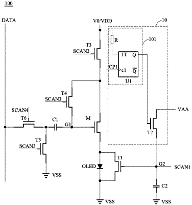
1. A pixel drive circuit, comprising:
a light-emitting element, wherein a first end of the light-emitting element is electrically coupled with a reference-voltage end, and the pixel drive circuit is configured to drive the light-emitting element to emit lights;
a drive transistor, electrically coupled with a second end of the light-emitting element;
a reset loop;
a first capacitor, wherein the first capacitor is coupled in series in the reset loop, a first end of the first capacitor is electrically coupled with a control end of the drive transistor, and the reset loop is conductive in a reset phase to receive a reset voltage, to charge the first capacitor to raise a voltage at the first end of the first capacitor, so as to reset a voltage at the control end of the drive transistor to the reset voltage through the first capacitor;
a first switch tube, coupled in parallel at two ends of the light-emitting element;
a second capacitor, wherein a first end of the second capacitor is electrically coupled with a control end of the first switch tube;
a pre-charge module, electrically coupled with the first end of the second capacitor, and configured to charge the second capacitor in the reset phase to raise a voltage at the first end of the second capacitor to a first voltage, wherein the first voltage is lower than a sum of a voltage at the reference-voltage end and a threshold voltage of the first switch tube; and
a threshold compensation loop, comprising the first capacitor, the drive transistor, and the first switch tube which are electrically coupled in series; wherein the second capacitor continues to be charged according to a first scan signal in a threshold compensation phase, such that a voltage at the control end of the first switch tube is raised continuously from the first voltage to switch on the first switch tube, so as to conduct the threshold compensation loop; wherein the first capacitor is discharged through the conductive threshold compensation loop, to make the voltage at the control end of the drive transistor drop from the reset voltage to a second voltage, the drive transistor enters into a critical on-state when the voltage at the control end of the drive transistor is equal to the second voltage, and the second voltage is lower than or equal to the reset voltage.
|
|
11. A display panel, comprising:
a substrate having a display region; and
a plurality of pixel drive circuits arranged in an array in the display region of the substrate, wherein the pixel drive circuit comprises:
a light-emitting element, wherein a first end of the light-emitting element is electrically coupled with a reference-voltage end, and the pixel drive circuit is configured to drive the light-emitting element to emit lights;
a drive transistor, electrically coupled with a second end of the light-emitting element;
a reset loop;
a first capacitor, wherein the first capacitor is coupled in series in the reset loop, a first end of the first capacitor is electrically coupled with a control end of the drive transistor, and the reset loop is conductive in a reset phase to receive a reset voltage, to charge the first capacitor to raise a voltage at the first end of the first capacitor, so as to reset a voltage at the control end of the drive transistor to the reset voltage through the first capacitor;
a first switch tube, coupled in parallel at two ends of the light-emitting element;
a second capacitor, wherein a first end of the second capacitor is electrically coupled with a control end of the first switch tube;
a pre-charge module, electrically coupled with the first end of the second capacitor, and configured to charge the second capacitor in the reset phase to raise a voltage at the first end of the second capacitor to a first voltage, wherein the first voltage is lower than a sum of a voltage at the reference-voltage end and a threshold voltage of the first switch tube; and
a threshold compensation loop, comprising the first capacitor, the drive transistor, and the first switch tube which are electrically coupled in series; wherein the second capacitor continues to be charged according to a first scan signal in a threshold compensation phase, such that a voltage at the control end of the first switch tube is raised continuously from the first voltage to switch on the first switch tube, so as to conduct the threshold compensation loop; wherein the first capacitor is discharged through the conductive threshold compensation loop, to make the voltage at the control end of the drive transistor drop from the reset voltage to a second voltage, the drive transistor enters into a critical on-state when the voltage at the control end of the drive transistor is equal to the second voltage, and the second voltage is lower than or equal to the reset voltage.
|