| CPC G09G 3/32 (2013.01) [G09G 2300/0842 (2013.01); G09G 2310/0278 (2013.01)] | 18 Claims |
|
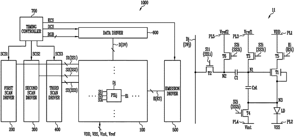
1. A display device comprising:
first to third scan lines;
an emission control line;
a data line;
a scan driver which supplies a first scan signal, a second scan signal, and a third scan signal to the first scan line, the second scan line, and the third scan line, respectively, in a first non-emission period, and supplies the second scan signal to the second scan line in a second non-emission period;
an emission driver which supplies an emission control signal to the emission control line in the first non-emission period and the second non-emission period;
a data driver which supplies a data signal to the data line in the first non-emission period; and
a pixel connected to the first to third scan lines, the emission control line and the data line and comprising:
a light-emitting element;
a first transistor which controls a driving current which flows from a first power line which provides a first supply voltage through the light-emitting element to a second power line which provides a second supply voltage based on a voltage of a first node;
a second transistor which is connected between the data line and a second node, and turned on in response to the first scan signal supplied to the first scan line;
a first capacitor connected between the first node and the second node;
a third transistor which is connected between a third power line which provides a third supply voltage and the first node, and turned on in response to the third scan signal supplied to the third scan line;
a storage capacitor connected between the first node and a third node;
a fourth transistor which is connected between the third node and a fourth power line which provides a fourth supply voltage, and turned on in response to the second scan signal supplied to the second scan line;
a fifth transistor which is connected between the first power line and the first transistor, and turned off in response to the emission control signal supplied to the emission control line; and
a sixth transistor which supplies a fifth supply voltage to the second node in response to the third scan signal,
wherein:
the sixth transistor is connected between the third power line and the second node, and
the fifth supply voltage is the third supply voltage.
|