| CPC G09G 3/32 (2013.01) [G09G 2300/0408 (2013.01); G09G 2300/0439 (2013.01); G09G 2310/0275 (2013.01)] | 20 Claims |
|
1. A display apparatus comprising:
a base substrate having a data line disposed on a first side thereof;
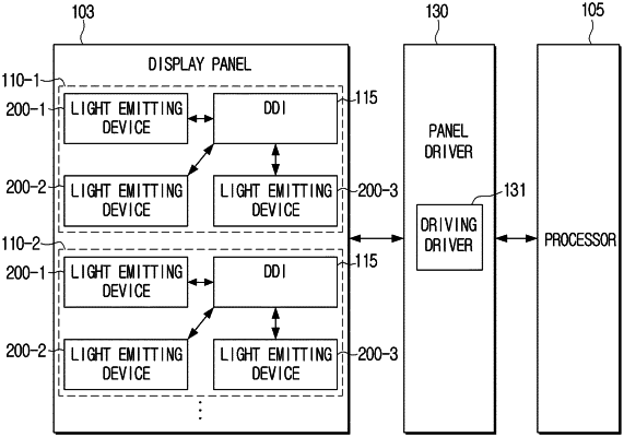
a plurality of pixel modules arranged in a matrix format on the first side of the base substrate; and
a driving driver configured to provide a data signal in a digital format through the data line to each of the plurality of pixel modules,
wherein each of the plurality of pixel modules comprises:
a light emitting layer in which a plurality of light emitting diode (LED) devices are disposed to form a pixel,
a driving layer comprising a display driver integrated circuit (DDI) formed below the light emitting layer configured to generate a driving signal to drive the plurality of LED devices, and
a substrate layer, formed between the driving layer and the base substrate, comprising a data input pad configured to receive the data signal and transmit the data signal to the DDI and a data output pad configured to provide the data signal to another adjacent pixel module.
|