| CPC G09G 3/32 (2013.01) [G09G 3/30 (2013.01); G09G 3/325 (2013.01); G09G 3/3208 (2013.01); G09G 3/3225 (2013.01); G09G 3/3233 (2013.01); G09G 2300/0819 (2013.01); G09G 2310/0267 (2013.01); G09G 2320/0233 (2013.01); G09G 2320/045 (2013.01)] | 18 Claims |
|
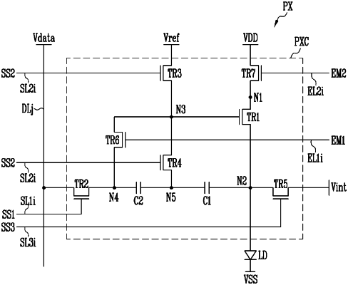
1. A display device comprising:
pixels connected to a first scan line, a second scan line, a third scan line, a data line, a first emission control line, and a second emission control line,
wherein each of the pixels comprises:
a light emitting element;
a first transistor connected between a first node coupled to a first power source and a second node coupled to an anode of the light emitting element, and including a gate electrode connected to a third node;
a second transistor directly connected between the data line and a fourth node, and including a gate electrode connected to the first scan line;
a first capacitor connected between the second node and a fifth node;
a second capacitor connected between the fourth node and the fifth node;
a third transistor directly connected between the third node and a third power source, and including a gate electrode directly connected to the second scan line;
a fourth transistor directly connected between the third node and the fifth node, and including a gate electrode connected to the second scan line; and
a sixth transistor connected between the third node and the fourth node, and including a gate electrode connected to the first emission control line.
|