| CPC G09G 3/006 (2013.01) [H10K 59/131 (2023.02)] | 20 Claims |
|
1. A display device comprising:
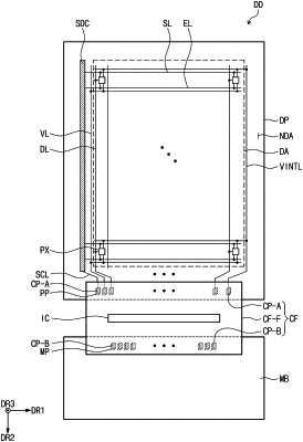
a display panel;
a main circuit board comprising a plurality of board pads arranged along a first direction;
a connection circuit board electrically connected to the display panel on one side thereof and electrically connected to the main circuit board on another side thereof; and
a driving chip disposed on the connection circuit board,
wherein the connection circuit board comprises:
a plurality of board connection pads respectively connected to the board pads;
a plurality of lines connecting the board connection pads and the driving chip to each other; and
a test pattern disposed spaced apart from the driving chip, and
wherein a first line and a second line among the lines are electrically connected to driving pads of the driving chip, and are electrically connected to the test pattern via the driving pads of the driving chip, and
wherein a same voltage is applied to the first line and the second line.
|