| CPC G06V 40/1318 (2022.01) [G09G 3/3233 (2013.01); H01L 27/14605 (2013.01); H01L 31/12 (2013.01); H10K 59/1216 (2023.02); H10K 59/40 (2023.02); H10K 59/60 (2023.02); H10K 59/65 (2023.02); G09G 2300/0426 (2013.01); G09G 2300/0842 (2013.01); G09G 2354/00 (2013.01)] | 29 Claims |
|
1. A display device comprising:
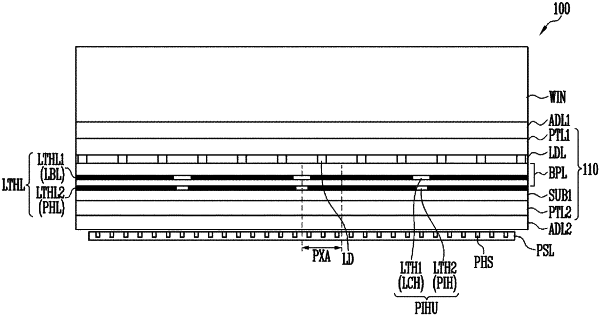
a first substrate comprising a plurality of pixel areas;
a circuit element layer disposed on a first surface of the first substrate, the circuit element layer comprising at least one conductive layer;
a light emitting element layer disposed on the circuit element layer;
a plurality of pixels each comprising:
a circuit element including at least one capacitor having at least one opening; and
a light emitting element disposed on the circuit element layer and the light emitting element layer in a corresponding one of the pixel areas;
a first light transmitting hole array layer comprising a plurality of first light transmitting holes distributed in the circuit element layer; and
a photo sensor array layer disposed on a second surface of the first substrate overlapping with the first light transmitting hole array layer, the photo sensor array layer comprising a plurality of photo sensors,
wherein each of the plurality of first light transmitting holes comprises a first opening and a second opening distributed in the at least one conductive layer,
wherein the at least one capacitor comprises:
a first capacitor electrode having the first opening; and
a second capacitor electrode overlapping with the first capacitor electrode and having the second opening,
wherein the first opening and the second opening have an identical width along one direction, and a length of the second opening extending in a direction intersecting the one direction is longer than a length of the first opening.
|