| CPC G06K 19/06028 (2013.01) [G02B 5/0284 (2013.01); G07D 7/0043 (2017.05)] | 10 Claims |
|
1. An optical assembly, comprising:
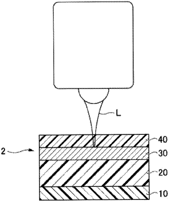
a spacer layer which is translucent or transparent;
an image forming reflector which has a reflective layer, the reflective layer being formed at least in a first region of the spacer layer; and
a protective layer which is laminated over the spacer layer and the image forming reflector, the protective layer being translucent or transparent, wherein
the spacer layer is made of a polyolefin or/and a polymer containing an aryl group,
the image forming reflector has a visible image formed therein, the visible image being authenticatable,
the image forming reflector has an individual information record in which a code is stored in form of a plurality of removed linear segments, the removed linear segments being formed by removing parts of the reflective layer, and
the image forming reflector has white level regions and a black level region in planar view of the image forming reflector, each of the white level regions having the removed linear segments formed therein, the black level region being interposed between the white level regions.
|