| CPC G06K 7/10297 (2013.01) [G06K 19/0723 (2013.01); H04N 1/32138 (2013.01); B41J 29/38 (2013.01); G03G 15/50 (2013.01)] | 18 Claims |
|
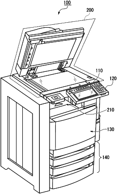
1. An image forming device, comprising:
a placement component configured to accommodate a sheet provided with a wireless tag;
a wireless tag communication writer configured to write information to the wireless tag provided on the sheet; and
a conductor provided in the placement component, the conductor configured to hinder communication between the wireless tag communication writer and the wireless tag, wherein the conductor comprises two or more conductors.
|