| CPC G06F 21/32 (2013.01) [G06F 3/0412 (2013.01); G06F 3/04164 (2019.05); G06V 40/1318 (2022.01)] | 7 Claims |
|
1. A semiconductor device, comprising:
a light-emitting device and an imaging device,
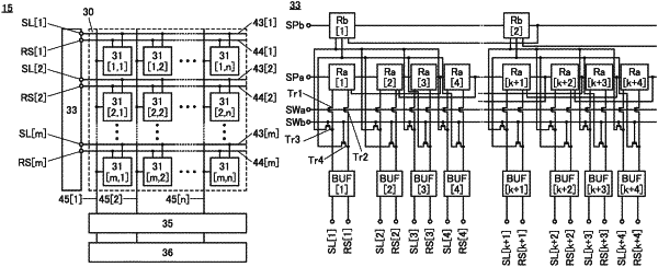
wherein the imaging device comprises a gate driver circuit and m rows of pixels,
wherein the gate driver circuit comprises a plurality of first register circuits and second register circuits whose number is less than that of the first register circuits,
wherein the first register circuits are connected with each other in series,
wherein the second register circuits are connected with each other in series,
wherein the gate driver circuit has a function of operating in a first mode and a second mode,
wherein in the first mode, the first register circuits are in an on state and the second register circuits are in an off state,
wherein in the second mode, the second register circuits are in the on state and the first register circuits are in the off state, and
wherein m is an integer more than or equal to 2.
|