| CPC G06F 11/1068 (2013.01) [G06F 3/0679 (2013.01); G06F 11/1044 (2013.01); G06F 11/1056 (2013.01)] | 20 Claims |
|
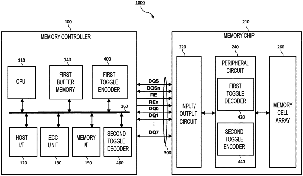
1. A memory system comprising:
a memory;
a controller that includes a first encoder configured to encode first data having a first bit length and a first number of toggles, into second data having a second bit length longer than the first bit length and a second number of toggles smaller than the first number of toggles; and
a bus including a plurality of signal lines between the memory and the controller,
wherein the signal lines include a first signal line through which the controller transmits the second data to the memory and a second signal line through which the controller transmits a signal to notify the memory of a timing for receiving the second data.
|