| CPC G06F 3/061 (2013.01) [G06F 3/0655 (2013.01); G06F 3/0676 (2013.01); G06F 3/0679 (2013.01); G06F 13/1668 (2013.01); G11C 7/10 (2013.01); G06F 2213/16 (2013.01)] | 20 Claims |
|
1. A method, comprising:
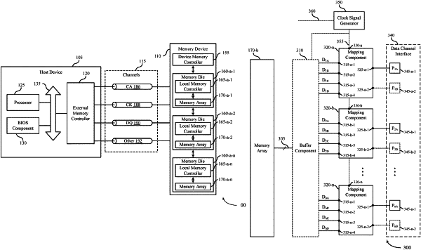
providing a memory die comprising:
a memory array having a plurality of memory cells;
a plurality of buffers configured to communicate logic state information with the memory array; and
a data channel interface comprising a plurality of pins configured to convey the logic state information, wherein the memory die supports a plurality of mappings between the plurality of buffers and a respective set of pins of the plurality of pins, the plurality of mappings comprising:
a first mapping that maps the plurality of buffers to a first quantity of the plurality of pins in accordance with a first burst length; and
a second mapping that maps the plurality of buffers to a second quantity of the plurality of pins in accordance with a second burst length, wherein the second quantity of pins is less than the first quantity of pins and the second burst length is greater than the first burst length; and
performing a configuration operation on the provided memory die to establish the first mapping or the second mapping.
|