| CPC G06F 3/061 (2013.01) [G06F 3/0634 (2013.01); G06F 3/0656 (2013.01); G06F 3/0659 (2013.01); G06F 3/0679 (2013.01); G06F 12/0875 (2013.01); G06F 13/16 (2013.01); G11C 7/1063 (2013.01); G11C 16/10 (2013.01); G11C 16/26 (2013.01); G06F 2212/1016 (2013.01); G06F 2212/214 (2013.01); G06F 2212/452 (2013.01); G06F 2212/7203 (2013.01); G06F 2212/7207 (2013.01); G11C 7/24 (2013.01)] | 12 Claims |
|
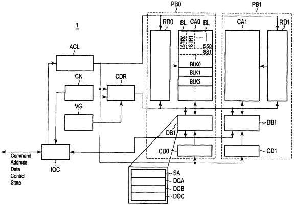
1. A memory system, comprising:
a semiconductor memory device including a first plane and a second plane, each of the first plane and the second plane including blocks; and
a memory controller configured to control the semiconductor memory device and to send a first command specifying an address in the first plane and a second command specifying an address in the second plane, wherein
the semiconductor memory device further includes:
a first cache configured to hold data transferred from the first plane;
a second cache configured to hold data transferred from the second plane; and
a controller configured to begin a first process on the first plane in response to the first command if the first and second caches are in the ready state when the first command is received and to begin a second process on the second plane according to the second command if at least the second cache is in the ready state,
the controller is further configured to determine whether a core operation associated with the second command can be performed simultaneously with a core operation associated with the first command if the second command is received while status information indicates the first cache is in the busy state and the second cache is in the ready state, the determination being made based on whether the core operation associated with the first command has started or not, and
the status information comprises a first status bit indicating whether the first plane is ready or busy and a second status bit indicating whether the second plane is ready or busy.
|