| CPC G06F 3/0445 (2019.05) [G02F 1/13338 (2013.01); G02F 1/133528 (2013.01); G02F 1/134363 (2013.01); G06F 3/044 (2013.01); G06F 3/0412 (2013.01); G06F 3/0416 (2013.01); G06F 3/0446 (2019.05); G06F 3/04164 (2019.05); G02F 1/134318 (2021.01); G06F 2203/04103 (2013.01); Y10T 29/49117 (2015.01)] | 16 Claims |
|
1. A display device comprising:
a display part; and
an input part; wherein
the display part including
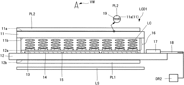
a first substrate,
a first polarizing plate on the first substrate, at least part of the first polarizing plate constituting a front surface of the display part,
a second substrate,
a second polarizing plate on the second substrate, at least part of the second polarizing plate constituting a back surface of the display part, and
a display area that includes a plurality of pixel electrodes, a common electrode and a display functional layer each of which is arranged between the first substrate and the second substrate, a display image formed by applying a display voltage between the plurality of pixel electrodes and the common electrode in a display period,
the input part including
a third substrate having a back surface facing the front surface of the display part,
a plurality of detection electrodes formed on the back surface of the third substrate,
a conductive layer provided between the back surface of the third substrate and the front surface of the display part, and
a first adhesive layer provided between the plurality of detection electrodes and the conductive layer,
each of the plurality of detection electrodes is glued to the conductive layer via the first adhesive layer,
the conductive layer overlaps the third substrate without through the plurality of the detection electrodes outside the display area, and
part of the plurality of the detection electrodes is uncovered by the conductive layer outside the display area.
|