| CPC G06F 3/041 (2013.01) [G06F 1/1626 (2013.01); G06F 1/1643 (2013.01); G06F 1/1684 (2013.01); G06F 1/1686 (2013.01)] | 19 Claims |
|
1. An electronic device, comprising:
a housing comprising a first surface facing in a first direction, a second surface facing in a second direction opposite to the first direction, and a transparent substrate forming at least a portion of the first surface;
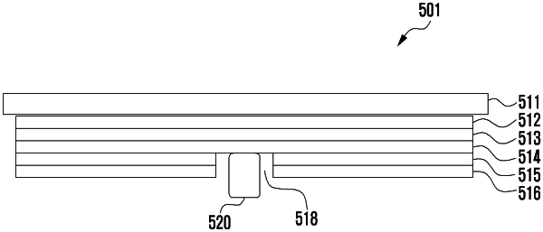
a display disposed between the transparent substrate and the second surface of the housing and configured to include a third surface facing in the first direction and a fourth surface facing in the second direction, wherein the display comprises a transmitting layer and a protective layer including an impact absorption pattern layer and a black layer;
the protective layer disposed between the transmitting layer and the second surface of the housing and configured to block a light emitted from the second direction, wherein a hole is formed in which at least a portion of the protective layer is removed and the hole is not formed in the transmitting layer; and
an image sensor configured to detect an external light passing through the transparent substrate, the display, and the hole formed in the protective layer, wherein the image sensor is disposed under the fourth surface of the display and between the fourth surface of the display and the second surface of the housing.
|