| CPC G06F 1/266 (2013.01) [G06F 13/4282 (2013.01); G06F 2213/0042 (2013.01)] | 19 Claims |
|
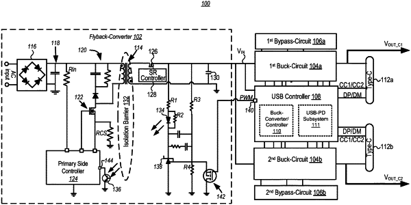
12. A universal serial bus power delivery (USB-PD) power adaptor comprising:
a flyback-converter;
a plurality of buck-circuits coupled between the flyback-converter and a plurality USB ports, each of the plurality of buck-circuits operable to receive a single input voltage (VIN) from the flyback-converter and to output a requested voltage to one of the plurality of USB ports;
a plurality of bypass circuits, each operable to bypass one of the plurality of buck-circuits and couple VIN from the flyback-converter directly to one of the plurality of USB ports; and
a USB controller coupled to the flyback-converter, the plurality of bypass circuits and the plurality of buck-circuits, the USB controller operable to operate the USB PD power adaptor in a variable-buck-input-mode,
wherein when a first USB port of the plurality of USB ports is connected to a first device, the USB controller is operable to:
operate the flyback-converter to generate and regulate a VIN equal to a first output voltage (VOUT_C1) requested by the first device; and
enable a first bypass circuit of the plurality of bypass circuits to bypass a first buck-circuit of the plurality of buck-circuits to couple VIN to the first USB port.
|