| CPC G05F 1/575 (2013.01) [H02M 1/0045 (2021.05); H02M 3/158 (2013.01)] | 20 Claims |
|
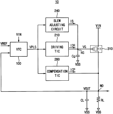
1. A low drop-out (LDO) regulator, comprising:
a voltage-to-time converter (VTC) responsive to a reference voltage and an output voltage, which is fed-back from an output node, said VTC configured to generate a voltage pulse signal having: (i) a sign associated with a magnitude of the output voltage relative to a magnitude of the reference voltage, and (ii) a first pulse width proportional to a difference in magnitude between the output voltage and the reference voltage;
a driving time-to-current converter (TIC) configured to drive a gate node with a non-zero driving current having a magnitude proportional to the first pulse width of the voltage pulse signal, in response to the sign of the voltage pulse signal indicating that the relative magnitude of the output voltage to the reference voltage has a non-zero value;
a slew adjusting circuit configured to drive the gate node with a non-zero slew adjusting current, in response to the first pulse width of the voltage pulse signal being equal to or greater than a reference time interval;
a pass transistor having a gate terminal electrically connected to the gate node, a first current carrying terminal responsive to an input voltage, and a second current carrying terminal electrically coupled to the output node; and
a compensation TIC configured to drive the output node with a non-zero compensation current having a magnitude proportional to the first pulse width of the voltage pulse signal, in response to the sign of the voltage pulse signal indicating that the relative magnitude of the output voltage to the reference voltage has a non-zero value.
|