US 11,740,563 B2
Mask cleaning
Shu-Hao Chang, Taipei (TW); Norman Chen, Hsinchu (TW); Jeng-Horng Chen, Hsinchu (TW); Kuo-Chang Kau, Yuanli Township (TW); Ming-Chin Chien, Hsinchu (TW); Shang-Chieh Chien, New Taipei (TW); Anthony Yen, Hsinchu (TW); and Kevin Huang, Hsinchu (TW)
Assigned to TAIWAN SEMICONDUCTOR MANUFACTURING COMPANY, LTD., Hsinchu (TW)
Filed by Taiwan Semiconductor Manufacturing Company, Ltd., Hsin-Chu (TW)
Filed on Feb. 22, 2022, as Appl. No. 17/677,183.
Application 17/677,183 is a continuation of application No. 16/660,640, filed on Oct. 22, 2019, granted, now 11,256,179.
Application 16/660,640 is a continuation of application No. 14/840,581, filed on Aug. 31, 2015, granted, now 10,459,352, issued on Oct. 29, 2019.
Prior Publication US 2022/0179326 A1, Jun. 9, 2022
This patent is subject to a terminal disclaimer.
Int. Cl. G03F 7/20 (2006.01); G03F 7/00 (2006.01)
CPC G03F 7/70866 (2013.01) [G03F 7/70925 (2013.01)] 20 Claims
OG exemplary drawing
 
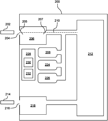
1. A lithography system comprising:
a first load lock chamber configured to receive a mask;
a cleaning module configured to clean the mask;
a second load lock chamber configured to receive a wafer; and
an exposure module configured to expose the wafer to a light source through use of the cleaned mask,
wherein a direct path is provided between the first load lock chamber and the exposure module allowing the first load lock chamber to directly couple to the exposure module without through the cleaning module.