| CPC G03F 1/36 (2013.01) [G03F 7/70441 (2013.01); G06F 30/398 (2020.01); G06F 2119/18 (2020.01)] | 20 Claims |
|
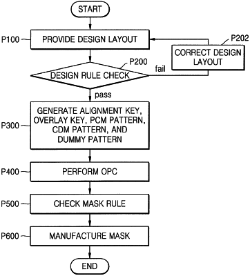
1. A method of manufacturing a lithographic mask, the method comprising:
providing a design layout including a plurality of patterns for manufacturing a semiconductor device;
performing an optical proximity correction (OPC) on the design layout for correcting an optical proximity effect (OPE), such that a corrected design layout is formed; and
forming the lithographic mask based on the corrected design layout,
wherein performing the OPC includes:
generating a plurality of segments by dividing edges of the plurality of patterns; and
adjusting a bias of the plurality of segments to form the corrected design layout,
wherein generating the plurality of segments includes:
determining, as first dissection positions, positions spaced apart by a first length from each of corners of the plurality of patterns,
determining, as second dissection positions, positions obtained by vertically or horizontally projecting each of the corners onto adjacent patterns,
determining third dissection positions along opposite ones of the edges of the plurality of patterns to adjust widths of the plurality of patterns,
performing a local uniform dissection for determining fourth dissection positions for each second length based on local coordinate systems using the corners as origins, and
performing a global uniform dissection for determining fifth dissection positions for each third length based on a global coordinate system that is a coordinate system of an entire design layout.
|