| CPC G02F 1/136286 (2013.01) [G02B 6/0083 (2013.01); G02F 1/1339 (2013.01); G02F 1/1368 (2013.01); G02F 1/13452 (2013.01); G02F 1/133345 (2013.01); G02F 1/136227 (2013.01); H01L 33/08 (2013.01); G02F 1/13458 (2013.01); H01L 2924/0002 (2013.01)] | 10 Claims |
|
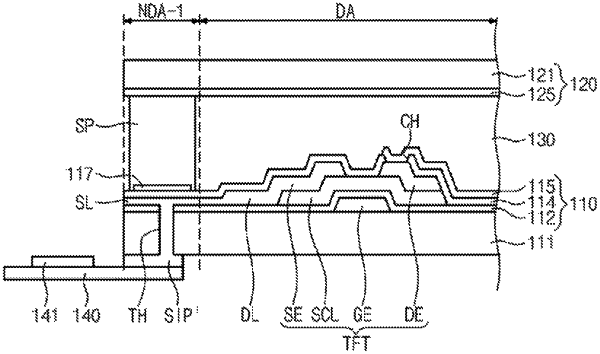
1. A display panel comprising:
a first substrate including a base substrate having a lower surface and an upper surface, a switching element disposed on the upper surface, a signal input pad, a signal line disposed on the upper surface and connecting the signal input pad to the switching element, and a protective layer disposed on the upper surface and overlapping the signal line;
a flexible printed circuit board disposed under the lower surface and connected to the signal input pad; and
a driver IC (Integrated Circuit) mounted on the flexible printed circuit board,
wherein data signals are transmitted from the driver IC to the switching element, and a portion of the signal input pad that is disposed between the lower surface and the flexible printed circuit board is exposed to an outside.
|