| CPC G02F 1/0147 (2013.01) [G02F 1/2257 (2013.01); G02F 1/212 (2021.01); G02F 2201/063 (2013.01)] | 20 Claims |

|
1. A method of manufacturing a semiconductor device,
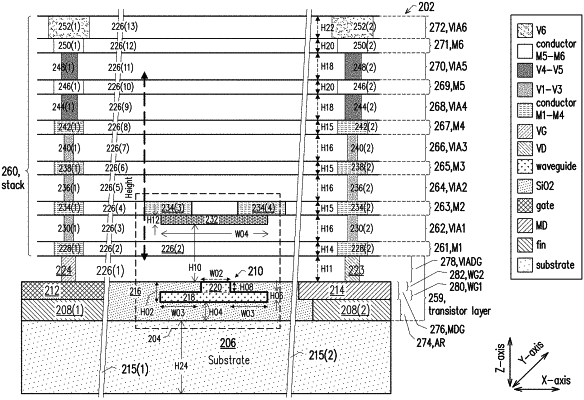
for a layout diagram stored on a non-transitory computer-readable medium and including a transistor level, a first level of metallization (M_1st level), a first level of interconnection (VIA_1st level) and a second level of metallization (M_2nd level) representing correspondingly a transistor layer, a first layer of metallization (M_1st layer), a first layer of interconnection (VIA_1st layer) and a second layer of metallization (M_2nd layer) in the semiconductor device,
the transistor level including a first waveguide level (WG_1st level), a second waveguide level (WG_2nd level) and a third level of interconnection (VIA_3rd level) representing correspondingly a first waveguide layer (WG_1st layer), a second waveguide layer (WG_2nd layer) and a third layer of interconnection (VIA_3rd layer),
the method comprising generating the layout diagram including:
generating component patterns correspondingly in one or more of the WG_1st level, WG_2nd level or the VIA_3rd level representing corresponding components of one or more transistors;
generating a first waveguide pattern in the WG_1st level;
generating a second waveguide pattern in the WG_2nd level;
locating the second waveguide pattern over the first waveguide pattern;
generating a heater pattern in the VIA_3rd level or the VIA_1st level; and
locating the heater pattern over the second waveguide pattern; and
the method further comprising at least one of:
(A) making one or more photolithographic exposure based on the layout diagram;
(B) fabricating one or more semiconductor masks based on the layout diagram; or
(C) fabricating at least one component in a layer of a semiconductor integrated circuit based on the layout diagram.
|