| CPC G02B 6/4214 (2013.01) [G02B 6/1221 (2013.01); G02B 6/4201 (2013.01); G02B 6/4204 (2013.01)] | 20 Claims |
|
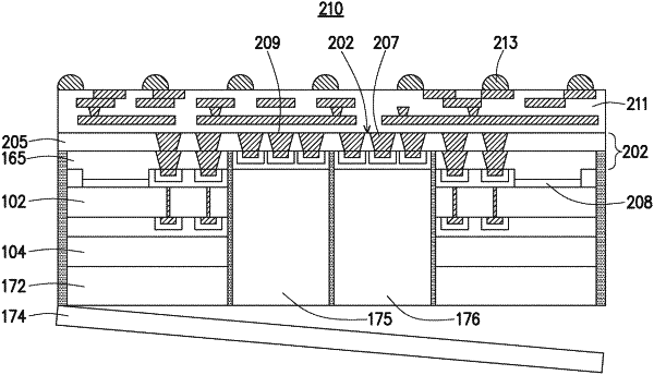
1. A silicon photonic (SiPh) structure comprising:
an electrical integrated circuit (EIC);
a photonic integrated circuit (PIC) disposed on top of the EIC;
at least one polymer waveguide (PWG) disposed on top of the PIC and forming a polymer bridging layer, wherein the at least one PWG comprises a core layer comprising a first polymer and at least two cladding layers comprising a second polymer that surrounds the core layer;
an integration fan-out redistribution (InFO RDL) layer disposed on top of the at least one PWG;
at least one optical lens configured to direct a light signal through the InFO RDL layer; and
a SiPh grating coupler comprising first and second grating structures, respectively, wherein light from the at least one optical lens is received by the first grating structure, which changes a direction of the light so that the light is collected by the second grating structure so as to direct light between the PIC and the at least one PWG.
|