| CPC G02B 6/12019 (2013.01) [H04B 10/43 (2013.01); H04B 10/6165 (2013.01)] | 19 Claims |
|
1. A circuit for detecting an optical data signal, the circuit comprising:
a photonics substrate;
a splitter configured to receive the optical data signal from an input port formed in the photonics substrate and output a first portion of the optical data signal and a second portion of the optical data signal;
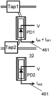
a first tap coupler configured to receive the first portion of the optical data signal;
a second tap coupler configured to receive the second portion of the optical data signal;
a first photodiode formed in the photonics substrate, the first photodiode configured to (i) receive, via the first tap coupler, the first portion of the optical data signal, (ii) receive, via the second tap coupler, the second portion of the optical data signal, and (iii) convert light power of the first portion and the second portion to generate a first current; and
a second photodiode formed in the photonics substrate without being coupled to any input port or waveguide, the second photodiode being configured to output a second current without receiving any portion of the optical data signal, the second current corresponding to a dark current induced in the second photodiode,
the circuit being configured to subtract the second current from the first current to generate an output signal corresponding to a photocurrent of the optical data signal without dark current induced in the first photodiode.
|