| CPC G01S 7/4863 (2013.01) [G01S 7/4865 (2013.01); H03K 3/037 (2013.01); G01S 17/89 (2013.01)] | 13 Claims |
|
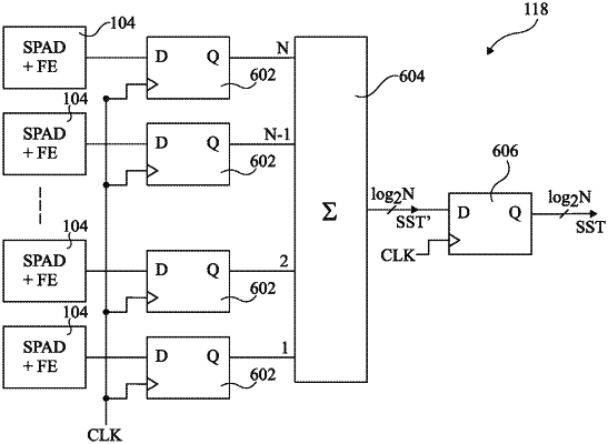
1. A combining network for an array of single-photon avalanche diode (SPAD) devices, comprising:
a plurality of synchronous sampling circuits, each synchronous sampling circuit being directly electrically connected to an output of a corresponding SPAD device and being configured to cause a logic high transition of its output at each rising edge of a clock signal where an output of the corresponding SPAD device is at a logic high at the rising edge as a result of a detection event but maintain its output at a logic low at each rising edge of the clock signal where the output of the corresponding SPAD device is not at a logic high at the rising edge as a result of a lack of a detection event;
a summation circuit directly electrically connected to an output of each of the synchronous sampling circuits and configured to count a number of logic high transitions at each rising edge of the clock signal to generate a binary output value representing the number of logic high transitions at that rising edge of the clock signal;
a multi-bit output flip-flop directly electrically connected to an output of the summation circuit to receive the binary output value; and
a histogram generation circuit directly electrically connected to an output of the multi-bit output flip-flop to receive the binary output value.
|