| CPC G01R 31/318536 (2013.01) [G01R 31/318541 (2013.01); G01R 31/318552 (2013.01); G01R 31/318555 (2013.01)] | 7 Claims |
|
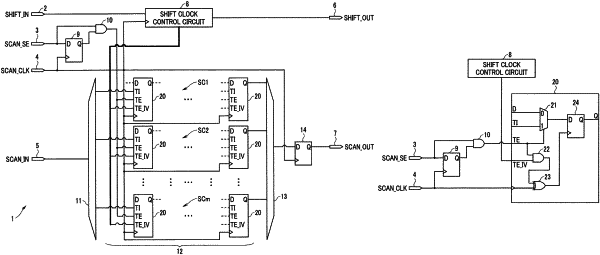
1. A semiconductor device comprising:
a plurality of scan chains each including a plurality of scan flip-flops;
a shift clock control circuit configured to output, to each of the plurality of scan chains, a control signal that non-inverts or inverts a scan clock signal; and
a shift clock generation circuit provided to each of the plurality of scan flip-flops and configured to generate a non-inverted scan clock signal or an inverted scan clock signal based on the control signal, the non-inverted scan clock signal being obtained by non-inverting the scan clock signal, the inverted scan clock signal being obtained by inverting the scan clock signal.
|