| CPC G01R 31/11 (2013.01) [H01L 23/528 (2013.01); H01L 23/562 (2013.01); H01L 23/585 (2013.01); H01L 24/06 (2013.01); H01L 2224/06131 (2013.01)] | 10 Claims |
|
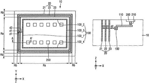
1. A semiconductor chip comprising:
a guard ring formed inside the semiconductor chip, extending from an upper surface of the semiconductor chip, and along an edge of the semiconductor chip,
wherein an internal region of the semiconductor chip and an external region of the semiconductor chip surrounding the internal region are defined by the guard ring;
a pad which is exposed on a surface of the semiconductor chip; and
an edge wiring disposed along an edge of the internal region in a form of a closed curve and connected to the pad,
wherein an incident wave is applied to the edge wiring through the pad, the incident wave forms a reflected wave upon the incident wave encountering a crack while traveling through the edge wiring, and a position of the crack is detected based on the reflected wave, and
wherein the edge wiring surrounds the pad in a plan view, and
a depth of the edge wiring is greater than a depth of the pad, based on a top surface of the semiconductor chip, in a cross-sectional view.
|