| CPC G01B 11/24 (2013.01) [G06T 7/60 (2013.01); G06V 10/267 (2022.01); H01J 37/28 (2013.01); H01J 2237/24578 (2013.01); H01J 2237/2803 (2013.01)] | 20 Claims |
|
1. A method of measuring a critical dimension (CD), comprising the steps of:
forming a plurality of patterns in a substrate;
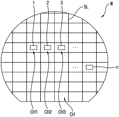
creating first to n-th images, wherein n is a natural number greater than 1, for first to n-th areas in the substrate, respectively, wherein the first to n-th areas do not overlap with each other, wherein each of the first to n-th areas includes at least some of the plurality of patterns;
creating a merged image from the first to n-th images; and
measuring a CD of a measurement object from the plurality of patterns using the merged image,
wherein the merged image has a higher resolution than each of the first to n-th images.
|