| CPC B32B 9/007 (2013.01) [B32B 37/18 (2013.01); B32B 38/0008 (2013.01); B32B 2038/0064 (2013.01); B32B 2310/14 (2013.01); B32B 2551/08 (2013.01)] | 23 Claims |
|
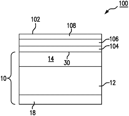
1. A wafer comprising:
a layer containing silicon;
a layer of polycrystalline diamond deposited on the layer containing silicon;
a polished silicon layer on the layer of polycrystalline diamond; and
a bow-compensation layer for reducing wafer-bow of the layer containing silicon and the layer of polycrystalline diamond; and
wherein the layer containing silicon is located between the layer of polycrystalline diamond and the bow-compensation layer, and
wherein the layer of polycrystalline diamond is located between the polished silicon layer and the layer containing silicon.
|