| CPC A61B 6/584 (2013.01) [G01T 1/16 (2013.01); B41F 16/00 (2013.01)] | 20 Claims |
|
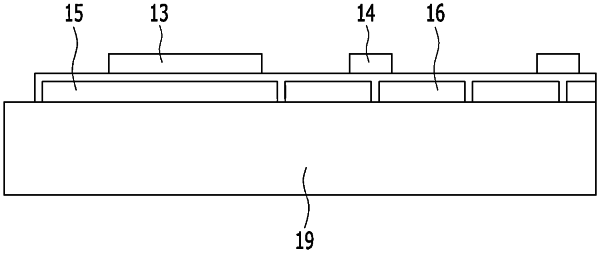
1. An X-ray detector comprising:
a photodiode layer formed on a base substrate within a pixel area and comprises a plurality of photodiode pixel units;
a dummy layer formed on the base substrate within a peripheral area and insulated from the plurality of photodiode pixel units;
a plurality of pixel driving integrated chips mounted on the photodiode layer;
a plurality of primary column and row integrated chips printed on the dummy layer; and
metal lines mounted on the pixel driving integrated chips and primary column and row integrated chips for coupling the column and row integrated chips with pixel driving integrated chips and other constituent elements,
wherein the plurality of pixel driving integrated chips and primary column and row integrated chips are manufactured separately from the photodiode layer and the dummy layer and attached on the photodiode layer and the dummy layer, respectively.
|