| CPC H10N 70/231 (2023.02) [G11C 13/0004 (2013.01); H10N 70/8828 (2023.02)] | 20 Claims |
|
1. A memory device, comprising:
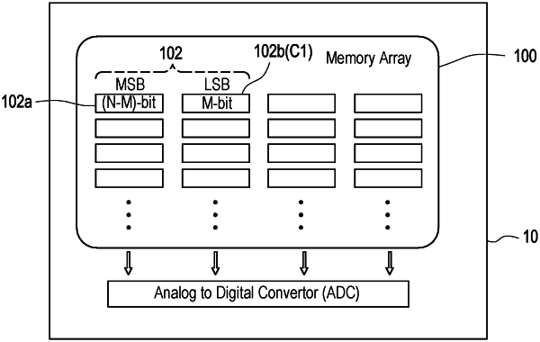
a memory array, comprising an N-bit memory unit forming one word in the memory array, wherein N is a positive integer of at least 5, and the N-bit memory unit comprises a least significant bit (LSB) part comprising M LSBs and a most significant bit (MSB) part comprising (N-M) MSB, wherein M is a positive integer of at least 4;
wherein the LSB part comprises:
a first memory cell, configured to store at least two bits, wherein the first memory cell is configured to store at least two first bits of the M LSBs;
a second memory cell, configured to store at least two bits, wherein the second memory cell is configured to store at least two second bits of the M LSBs, wherein the second memory cell is a phase change memory cell, and a material of the phase change memory cell is GST with a specific percentage of Nitrogen doping; and
wherein the MSB part comprises:
at least one third memory cell, configured to store only one bit, wherein the at least one third memory cell is configured to store the (N-M) MSB.
|