| CPC H10N 60/815 (2023.02) [H01L 24/08 (2013.01); H01L 24/80 (2013.01); H10N 60/0912 (2023.02); H10N 60/12 (2023.02); H10N 60/805 (2023.02); H10N 69/00 (2023.02); H01L 2224/08146 (2013.01); H01L 2224/80895 (2013.01); H01L 2224/80896 (2013.01)] | 20 Claims |

|
1. An integrated circuit comprising:
a first substrate having a plurality of conductive contact pads spaced apart from one another on a surface of the first substrate;
a dielectric layer overlying the first substrate and the plurality of conductive contact pads;
a second substrate overlying the dielectric layer, and
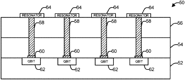
a plurality of superconducting contacts extending through the second substrate and the dielectric layer to the first substrate, wherein each superconducting contact of the plurality of superconducting contacts is aligned with and in contact with a respective conductive contact pad of the plurality of conductive contact pads, wherein the integrated circuit further comprises a first qubit and a second qubit disposed within the first substrate, wherein a first of the plurality of conductive contact pads is coupled to the first qubit and a second of the plurality of conductive contact pads is coupled to the second qubit.
|