US 12,069,965 B2
Method for manufacturing memory device
Ya-Jui Tsou, Taichung (TW); Zong-You Luo, Taoyuan (TW); Chee-Wee Liu, Taipei (TW); Shao-Yu Lin, Taichung (TW); Liang-Chor Chung, Hsinchu County (TW); and Chih-Lin Wang, Hsinchu County (TW)
Assigned to TAIWAN SEMICONDUCTOR MANUFACTURING CO., LTD., Hsinchu (TW); and NATIONAL TAIWAN UNIVERSITY, Taipei (TW)
Filed by TAIWAN SEMICONDUCTOR MANUFACTURING CO., LTD., Hsinchu (TW); and NATIONAL TAIWAN UNIVERSITY, Taipei (TW)
Filed on Jul. 17, 2023, as Appl. No. 18/353,569.
Application 18/353,569 is a continuation of application No. 17/525,927, filed on Nov. 14, 2021, granted, now 11,778,923.
Application 17/525,927 is a continuation of application No. 16/443,772, filed on Jun. 17, 2019, granted, now 11,177,430, issued on Nov. 16, 2021.
Prior Publication US 2023/0363287 A1, Nov. 9, 2023
Int. Cl. H10N 50/80 (2023.01); G11C 11/16 (2006.01); H10B 61/00 (2023.01); H10N 50/01 (2023.01)
CPC H10N 50/80 (2023.02) [G11C 11/161 (2013.01); H10B 61/00 (2023.02); H10N 50/01 (2023.02)] 20 Claims
OG exemplary drawing
 
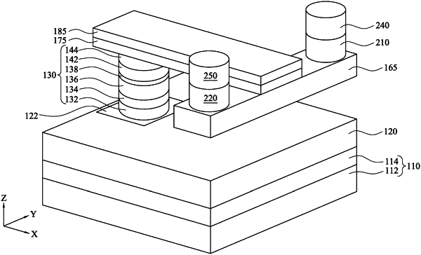
1. A method comprising:
forming a memory stack over a substrate;
depositing a dielectric layer to cover the memory stack;
forming an opening in the dielectric layer, wherein the opening does not expose the memory stack;
forming a spin-orbit-torque (SOT) layer in the opening; and
forming a free layer over the dielectric layer to interconnect the memory stack and the SOT layer.