| CPC H10N 50/80 (2023.02) [H10B 61/00 (2023.02); H10N 50/01 (2023.02); H10N 50/85 (2023.02)] | 20 Claims |

|
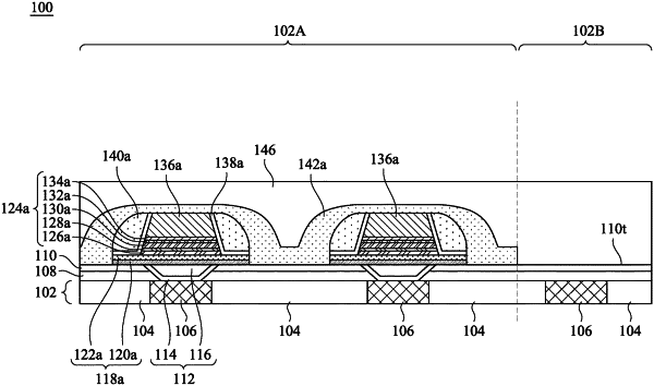
1. A magnetic random access memory (MRAM) device, comprising:
a substrate comprising a first inter-layer dielectric (ILD) layer having a metal line;
a first bottom electrode over the metal line;
a first MTJ stack over the first bottom electrode, comprising:
a pinned layer;
a tunnel barrier layer over the pinned layer; and
a free layer over the tunnel barrier layer;
a first spacer surrounding sidewalls of the first MTJ stack;
a topography-smoothing layer extending over a top surface of the first ILD layer, along a sidewall of the first bottom electrode and along a sidewall of the first spacer, wherein the topography-smoothing layer has a top portion over the first MTJ stack and a first side portion laterally surrounding the first spacer, and the first side portion has a maximal lateral thickness greater than a maximal vertical thickness of the top portion; and
a second inter-layer dielectric (ILD) layer over the topography-smoothing layer, wherein the second ILD layer has a material different from a material of the topography-smoothing layer.
|