| CPC H10N 50/10 (2023.02) [H10B 61/00 (2023.02); H10N 50/01 (2023.02); H10N 50/80 (2023.02); H10N 50/85 (2023.02)] | 18 Claims |

|
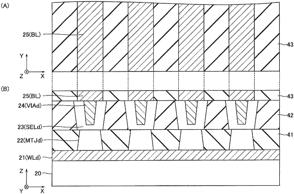
1. A magnetic memory device, comprising:
a first magnetoresistance effect element provided above a substrate; and
a first switching element member and a first conductor, each provided above the first magnetoresistance effect element,
wherein:
the first switching element member includes a first portion in contact with a lower surface of the first conductor directly above the first magnetoresistance effect element,
an area of a lower surface of the first switching element member is smaller than a cross-sectional area of the first switching element member along the lower surface of the first conductor,
the first switching element member further includes a second portion in contact with a side surface of the first conductor,
an area of the lower surface of the first conductor is smaller than the cross-sectional area, and
the area of the lower surface of the first conductor is smaller than an area of an upper surface of the first magnetoresistance effect element.
|