US 12,069,936 B2
Electronic device and method for slot-die depositing layers of the same
Anand Verma, Bihar (IN); David Martineau, Etoy (CH); Frank Nüesch, Wangen (CH); Jacob Heier, Zürich (CH); and Tobias Meyer, Féchy (CH)
Assigned to EMPA EIDGENÖSSISCHE MATERIALPRÜFUNGS-UND FORSCHUNGSANSTALT, Dubendorf (CH); and SOLARONIX S.A., Aubonne (CH)
Appl. No. 17/056,331
Filed by EMPA EIDGENÖSSISCHE MATERIALPRÜFUNGS-UND FORSCHUNGSANSTALT, Dubendorf (CH); and SOLARONIX S.A., Aubonne (CH)
PCT Filed May 17, 2019, PCT No. PCT/EP2019/062888
§ 371(c)(1), (2) Date Nov. 17, 2020,
PCT Pub. No. WO2019/219952, PCT Pub. Date Nov. 21, 2019.
Claims priority of application No. 18173055 (EP), filed on May 17, 2018; and application No. 18180245 (EP), filed on Jun. 27, 2018.
Prior Publication US 2021/0210685 A1, Jul. 8, 2021
Int. Cl. H10K 71/15 (2023.01); H10K 30/00 (2023.01); H10K 30/35 (2023.01); H10K 71/13 (2023.01)
CPC H10K 71/15 (2023.02) [H10K 30/35 (2023.02); H10K 30/451 (2023.02); H10K 71/135 (2023.02)] 16 Claims
OG exemplary drawing
 
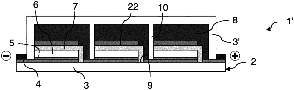
1. A method for depositing one or more layers of an optoelectronic device, the method comprising:
depositing one or more formulation by slot-die deposition, wherein said one or more formulation comprises:
one or more selected from the group consisting of: nanoparticles of a metal oxide material, metal-organic precursors of said metal oxide material, and carbon; and,
a carrier composition comprising a solvent mixture comprising one or more low boiling point solvent and one or more high boiling point solvent, wherein said one or more low boiling point solvent has a boiling point of <200° C. and said one or more high boiling point solvent has a boiling point of ≥200° ° C.