| CPC H10K 59/60 (2023.02) [G06V 40/1318 (2022.01); H10K 50/865 (2023.02); H10K 59/122 (2023.02); H10K 59/40 (2023.02)] | 17 Claims |

|
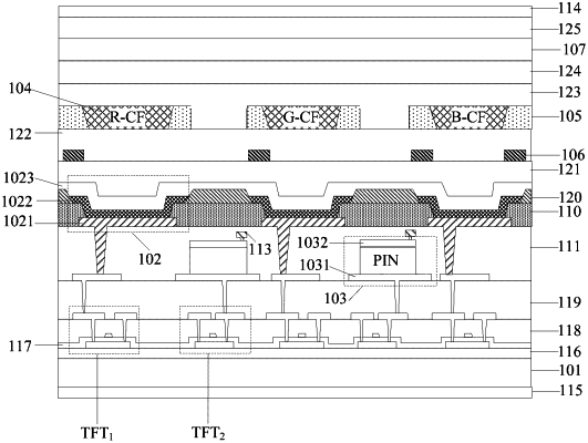
1. A display substrate, comprising:
a base substrate;
a plurality of light emitting devices, located on the base substrate;
a plurality of photosensitive devices, located between a layer where the plurality of light emitting devices are located and the base substrate, wherein an orthographic projection of each of the photosensitive devices on the base substrate is located at a gap between orthographic projections of adjacent light emitting devices on the base substrate;
a plurality of color resistors and a black matrix, located on a side of the layer where the plurality of light emitting devices are located facing away from the base substrate, wherein the black matrix has a plurality of first openings and a plurality of second openings, the plurality of color resistors are correspondingly disposed in the plurality of first openings and cover the plurality of light emitting devices, and orthographic projections of the plurality of second openings on the base substrate mutually overlap with the orthographic projections of the plurality of photosensitive devices on the base substrate;
a touch control structure, located between the layer where the plurality of light emitting devices are located and a layer where the black matrix is located, wherein an orthographic projection of the touch control structure on the base substrate is located in an orthographic projection of the black matrix on the base substrate, and the orthographic projection of the touch control structure on the base substrate does not overlap with the orthographic projections of the second openings on the base substrate; and
an ultrathin glass cover plate, a whole face of which being disposed on a side of the layer where the black matrix is located facing away from the base substrate;
wherein at least one of the second openings and one of the photosensitive devices are correspondingly disposed;
wherein one of the second openings and one of the photosensitive devices are correspondingly disposed, and the orthographic projection of the one of the second openings on the base substrate completely coincides with the orthographic projection of the corresponding one of the photosensitive devices on the base substrate; and
wherein a light receiving angle θ determined by the black matrix meets a following relationship: tan θ=d/h2=Px/(2h1), wherein d is a pore diameter of the one of the second openings, h1 is a distance between the ultrathin glass cover plate and the layer where the black matrix is located, h2 is a distance between the layer where the black matrix is located and a layer where the photosensitive devices are located, and Px is a distance between adjacent ridges or adjacent valleys of a fingerprint.
|