| CPC H10K 59/131 (2023.02) [H10K 59/122 (2023.02); H10K 59/1201 (2023.02)] | 10 Claims |

|
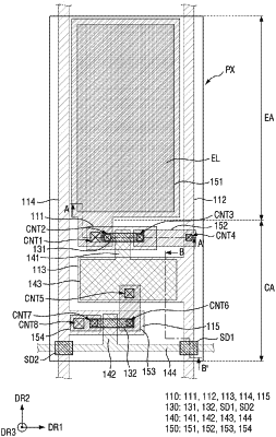
1. A display device including a storage capacitor and at least one transistor including a first semiconductor pattern, the display device comprising:
a substrate;
a first conductive layer disposed on the substrate and including a first electrode of the storage capacitor and a first signal line;
a buffer layer disposed on the first conductive layer;
a semiconductor layer disposed on the buffer layer and including the first semiconductor pattern and a second semiconductor pattern separated from the first semiconductor pattern;
an insulating layer disposed on the semiconductor layer; and
a second conductive layer disposed on the insulating layer and including a gate electrode of the transistor, a second electrode of the storage capacitor, and a second signal line;
wherein the first signal line and the second signal line overlap each other at least in a partial region in a thickness direction,
wherein at least a portion of the second semiconductor pattern is disposed in an overlap region where the first signal line and the second signal line overlap each other, and
wherein in the overlap region, a distance in the thickness direction between the first signal line and the second signal line is greater than a distance in the thickness direction between the first electrode and the second electrode of the storage capacitor.
|