| CPC H10K 59/131 (2023.02) [H10K 71/00 (2023.02); H10K 59/1201 (2023.02); H10K 77/111 (2023.02); H10K 2102/311 (2023.02); H10K 2102/351 (2023.02)] | 11 Claims |

|
1. A display device comprising:
a resin substrate having flexibility; and
a thin film transistor layer including a plurality of thin film transistors, the thin film transistor layer being provided on the resin substrate,
the thin film transistor layer further including a first inorganic insulating film including a first inorganic insulating layer, a second inorganic insulating film including a second inorganic insulating layer provided on the first inorganic insulating film, and a lead-out wiring line provided on the second inorganic insulating film,
the display device being provided with a display region configured to display an image generated by the plurality of thin film transistors, and a frame region located on a periphery of the display region,
the frame region including a bending portion that is bent around a bending axis extending in a first direction,
the bending portion being provided with a slit extending in the first direction in the thin film transistor layer,
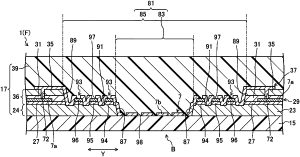
the slit comprising a first slit formed in the first inorganic insulating film and a second slit formed in the second inorganic insulating film with a width wider than a width of the first slit,
portions of the first inorganic insulating film on both sides in a width direction of the first slit forming step portions that are exposed from the second inorganic insulating film inside the second slit,
the lead-out wiring line being electrically connected to the thin film transistor layer, and extending from one side of the slit to the other side of the slit in a second direction intersecting with the first direction through the step portions,
wherein the step portions are provided with a protruding portion having an island shape, and
the lead-out wiring line includes an opening covering a perimeter edge surface of the protruding portion and exposing an upper face of the protruding portion.
|