| CPC H10K 59/131 (2023.02) [H01L 27/1222 (2013.01); H01L 27/124 (2013.01); H10K 59/121 (2023.02); H10K 71/00 (2023.02)] | 20 Claims |

|
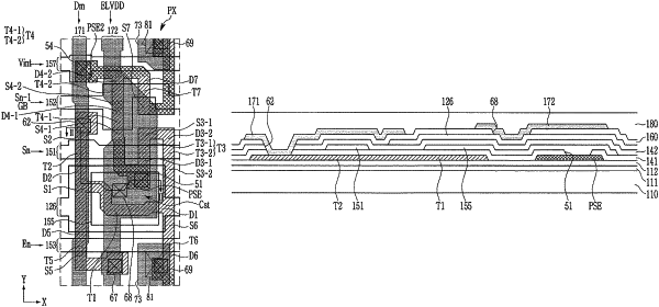
1. A manufacturing method of an organic light emitting diode display, comprising:
forming a semiconductor layer on a substrate;
forming a doping mask on the semiconductor layer and doping the semiconductor layer;
removing the doping mask;
forming a first insulation layer covering the semiconductor layer;
forming a first conductor on the first insulation layer;
doping the semiconductor layer by using the first conductor as a mask;
forming a second insulation layer covering the first conductor;
forming a second conductor on the second insulation layer;
forming a third insulation layer covering the second conductor;
forming a third conductor on the third insulation layer;
forming a passivation layer covering the third conductor; and
forming a pixel electrode on the passivation layer.
|