| CPC H10K 59/131 (2023.02) [H10K 50/865 (2023.02)] | 19 Claims |
|
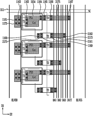
1. A display device comprising:
a substrate;
a first conductive layer disposed on the substrate;
a first insulating layer disposed on the first conductive layer;
a semiconductor layer disposed on the first insulating layer;
a second insulating layer disposed on the semiconductor layer;
a second conductive layer disposed on the second insulating layer and overlapping the semiconductor layer;
a third insulating layer disposed on the second conductive layer;
a third conductive layer disposed on the third insulating layer and including a common voltage transmitting portion overlapping the first conductive layer and transmitting a common voltage, wherein
the first conductive layer includes two end portions separated by a region of the first conductive layer,
the two end portions of the first conductive layer are electrically connected by a first connecting part, and
the region is disposed between the semiconductor layer and the common voltage transmitting portion.
|