| CPC H10K 59/131 (2023.02) [H10K 59/122 (2023.02); H10K 59/124 (2023.02); H10K 59/353 (2023.02); G09G 3/30 (2013.01); G09G 2300/0426 (2013.01)] | 19 Claims |

|
1. A display panel, comprising:
a base substrate, comprising a plurality of sub pixels;
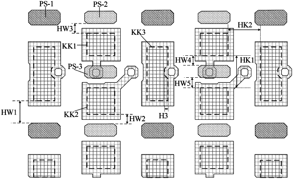
a first electrode layer, located on the base substrate and comprising anodes located in all the sub pixels, wherein each of the anodes comprises a main body part and a via hole part which are electrically connected with each other;
a pixel defining layer, located on one side of the first electrode layer facing away from the base substrate, wherein the pixel defining layer comprises openings located in all the sub pixels, and an orthographic projection of an opening on the base substrate is located in an orthographic projection of the main body part in each of the sub pixels on the base substrate; and
a supporting layer, located on one side of the pixel defining layer facing away from the base substrate; wherein
the supporting layer comprises a plurality of columns of first spacers and a plurality of columns of second spacers; the first spacers and the second spacers are located on different columns; one column of the first spacers corresponds to one column of the sub pixels, and one column of the second spacers corresponds to the other column of the sub pixels; a quantity of the sub pixels in the columns where the first spacers are located is different from a quantity of the sub pixels in the columns where the second spacers are located;
an anode of at least one of the sub pixels corresponding to the first spacers extends in a first direction, and the first spacers and the second spacers extend in a second direction respectively;
as for the first spacers and corresponding sub pixels, the first spacers and the corresponding sub pixels are arranged alternately and repeatedly in a column direction and correspond in a one-to-one mode;
an orthographic projection of the first spacers in the column direction does not overlap with an orthographic projection of the anodes in all the sub pixels in the column direction; and
a first ratio is formed between an area of the first spacers and an area of the openings of the corresponding sub pixels, a second ratio is formed between an area of the second spacers and an area sum of the openings of all the sub pixels between two adjacent second spacers in the column direction, and the first ratio is different from the second ratio;
wherein the sub pixels corresponding to the second spacers comprise first-color sub pixels and second-color sub pixels, and an anode of one first-color sub pixel and an anode of one second-color sub pixel are disposed between the second spacers adjacent in the column direction; and
the sub pixels corresponding to the first spacers comprise third-color sub pixels, and an anode of one third-color sub pixel is disposed between the first spacers adjacent in the column direction.
|