| CPC H10K 59/131 (2023.02) [H01R 4/04 (2013.01); H01R 12/62 (2013.01); H05K 1/09 (2013.01); H05K 1/118 (2013.01); H05K 1/189 (2013.01); H05K 3/328 (2013.01); H05K 2201/10128 (2013.01); H05K 2203/0292 (2013.01); H05K 2203/1377 (2013.01)] | 11 Claims |

|
1. A display device comprising:
a display module comprising a base substrate, the base substrate having a display area and a non-display area adjacent to the display area, and a first pad on the base substrate and overlapping the non-display area; and
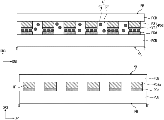
a circuit board comprising a first board and a second pad on the first board, the second pad electrically contacting the first pad, wherein the second pad is a single layer consisting of a single material comprising copper, wherein the second pad is directly on the first pad, and wherein the circuit board further comprises a third pad separated from the second pad on a plane of the circuit board and electrically connected to the second pad;
a driving circuit board comprising a second board and a driving pad on the second board, wherein the driving circuit board is electrically connected to the third pad; and
an anisotropic conductive film electrically connecting the third pad and the driving pad, the anisotropic conductive film comprises:
an adhesive film between the first board and the second board; and
conductive particles in the adhesive film and configured to electrically connect the third pad and the driving pad,
the third pad comprises:
a second metal layer on the first board; and
an auxiliary metal layer on the second metal layer and configured to electrically contact the conductive particles,
wherein the second metal layer is composed of the same material as that of the second pad.
|