| CPC H10K 59/123 (2023.02) [H10K 59/1213 (2023.02); H01L 27/124 (2013.01)] | 30 Claims |

|
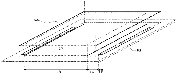
1. A light emitting diode display apparatus, comprising:
a substrate;
a driving element region which is formed on the substrate and in which a plurality of driving elements are arranged in a matrix form; and
an emitting element region in which a plurality of emitting elements are arranged in a matrix form, wherein each emitting element of the plurality of emitting elements includes a first electrode that is electrically connected to a corresponding driving element of the plurality of driving elements, a second electrode corresponding to the first electrode, and an emitting layer located between the first electrode and the second electrode,
wherein an area of the emitting element region is greater than an area of the driving element region, and
wherein a number of the plurality of emitting elements included in the emitting element region is great than a number of the plurality of driving elements included in the driving element region.
|