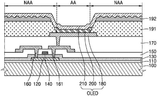
| CPC H10K 59/122 (2023.02) [H10K 71/191 (2023.02); G09G 3/3233 (2013.01); H10K 59/1201 (2023.02)] | 8 Claims |

|
1. A method of manufacturing a display apparatus, the method comprising:
preparing a substrate;
forming a pixel electrode on the substrate;
forming a pixel defining layer on the pixel electrode, the pixel defining layer having an opening that exposes a central portion of the pixel electrode; and
forming a liquid-repellent layer on the pixel defining layer, the liquid-repellent layer including an upper surface having a concavo-convex structure,
wherein the forming of the liquid-repellent layer comprises:
forming an organic material layer including an organic material for forming the pixel defining layer mixed with a first liquid-repellent agent and a second liquid-repellent agent having different surface energies from each other;
baking the organic material layer and phase-separating the pixel defining layer, the first liquid-repellent agent, and the second liquid-repellent agent such that the first liquid-repellent agent and the second liquid-repellent agent are located on the pixel defining layer;
irradiating plasma to remove a liquid-repellent layer remaining on an upper surface of the pixel electrode; and
baking the pixel defining layer after the irradiating the plasma.
|