US 12,069,898 B2
Display panel, manufacturing method thereof and display device
Qun Ma, Beijing (CN); Yue Wei, Beijing (CN); Mingxi Pan, Beijing (CN); and Haoming Lv, Beijing (CN)
Assigned to CHENGDU BOE OPTOELECTRONICS TECHNOLOGY CO., LTD., Sichuan (CN); and BOE TECHNOLOGY GROUP CO., LTD., Beijing (CN)
Appl. No. 17/287,900
Filed by CHENGDU BOE OPTOELECTRONICS TECHNOLOGY CO., LTD., Sichuan (CN); and BOE TECHNOLOGY GROUP CO., LTD., Beijing (CN)
PCT Filed Sep. 22, 2020, PCT No. PCT/CN2020/116768
§ 371(c)(1), (2) Date Apr. 22, 2021,
PCT Pub. No. WO2021/109682, PCT Pub. Date Jun. 10, 2021.
Claims priority of application No. 201911213367.0 (CN), filed on Dec. 2, 2019.
Prior Publication US 2022/0310721 A1, Sep. 29, 2022
Int. Cl. H10K 59/122 (2023.01); H10K 50/842 (2023.01); H10K 59/12 (2023.01); H10K 71/00 (2023.01)
CPC H10K 59/122 (2023.02) [H10K 50/8428 (2023.02); H10K 71/00 (2023.02); H10K 59/1201 (2023.02)] 20 Claims
OG exemplary drawing
 
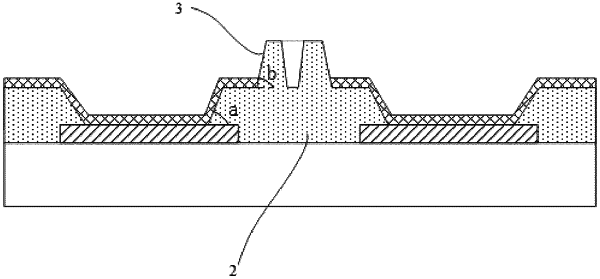
1. A display panel, comprising a base substrate, a thin film transistor (TFT) array arranged on the base substrate, a pixel definition layer arranged at a side of the TFT array away from the base substrate, and a plurality of light-emitting units arranged at a pixel region defined by the pixel definition layer, wherein the display panel further comprises a plurality of spacers arranged on a surface of the pixel definition layer away from the base substrate, a surface of at least one spacer away from the base substrate comprises a first portion and a second portion, a distance between the second portion and the base substrate is smaller than a distance between the first portion and the base substrate; wherein a slope angle of the pixel definition layer is not larger than 30°, and a slope angle of each spacer is not smaller than 40°.