| CPC H10K 59/1213 (2023.02) [H01L 27/1222 (2013.01); H01L 27/124 (2013.01); H10K 59/121 (2023.02); H10K 59/131 (2023.02); H10K 59/352 (2023.02); H10K 59/353 (2023.02); H10K 59/38 (2023.02)] | 11 Claims |
|
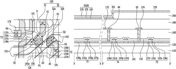
1. An organic light-emitting diode (OLED) display, comprising:
a substrate;
a semiconductor layer on the substrate;
a scan line transmitting a scan signal and extending in a first direction on the semiconductor layer;
an insulating layer on the scan line and having a contact hole overlapping the semiconductor layer;
a data line transmitting a data signal and extending in a second direction perpendicular to the first direction on the insulating layer;
a driving connector on the insulating layer and electrically connected to the semiconductor layer via the contact hole; and
an OLED on the data line,
wherein, in a plan view, the semiconductor layer includes a first semiconductor portion extending in the first direction, a second semiconductor portion extending in the second direction, and a third semiconductor portion between the first semiconductor portion and the second semiconductor portion and directly connected to the first semiconductor portion and the second semiconductor portion,
wherein the third semiconductor portion has a shorter side extending only in a third direction different from the first direction and the second direction, one end of the shorter side being directly connected to the first semiconductor portion and another end of the shorter side being directly connected to the second semiconductor portion,
wherein the third semiconductor portion has an expansion part protruding from the shorter side in a fourth direction crossing the third direction and having a maximum width, measured in the fourth direction, greater than a maximum width of the first semiconductor portion, measured in the second direction, and a maximum width of the second semiconductor portion, measured in the first direction, and
wherein the contact hole overlaps the expansion part, and the driving connector electrically connects a gate electrode of a driving transistor to the expansion part via the contact hole.
|