| CPC H10K 59/1213 (2023.02) [H01L 29/7869 (2013.01); H10K 59/1216 (2023.02)] | 25 Claims |

|
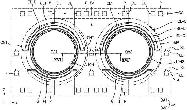
1. A display panel comprising:
a substrate comprising a first opening and a second opening that are spaced apart from each other;
a plurality of pixels located in a display area around the first opening and the second opening, each of the plurality of pixels comprising a pixel circuit comprising a first thin-film transistor and a display element connected to the pixel circuit;
a bottom metal layer located between the substrate and the first thin-film transistor;
emission control lines located on the substrate, extending in a first direction, and spaced apart from each other by the first opening and the second opening; and
a first conductive layer located in an intermediate area surrounding each of the first opening and the second opening to bypass the first opening and the second opening,
wherein the first conductive layer electrically connects the emission control lines that are spaced apart from each other by the first opening and the second opening, and the first conductive layer comprises a same material as a material of the bottom metal layer.
|