US 12,069,895 B2
Display Apparatus having shielding electrode overlapping connection line
Jieun Lee, Yongin-si (KR); Minchae Kwak, Yongin-si (KR); Byungsun Kim, Yongin-si (KR); Ilgoo Youn, Yongin-si (KR); Seunghan Jo, Yongin-si (KR); Junyoung Jo, Yongin-si (KR); and Minhee Choi, Yongin-si (KR)
Assigned to SAMSUNG DISPLAY CO., LTD., Yongin-si (KR)
Filed by SAMSUNG DISPLAY CO., LTD., Yongin-si (KR)
Filed on Dec. 6, 2021, as Appl. No. 17/457,732.
Application 17/457,732 is a continuation of application No. 16/938,087, filed on Jul. 24, 2020, granted, now 11,195,893.
Claims priority of application No. 10-2019-0090497 (KR), filed on Jul. 25, 2019.
Prior Publication US 2022/0093713 A1, Mar. 24, 2022
This patent is subject to a terminal disclaimer.
Int. Cl. H01L 29/12 (2006.01); H10K 59/121 (2023.01); H10K 59/126 (2023.01); H10K 59/131 (2023.01); H01L 27/12 (2006.01)
CPC H10K 59/1213 (2023.02) [H10K 59/1216 (2023.02); H10K 59/126 (2023.02); H10K 59/131 (2023.02); H01L 27/1225 (2013.01)] 30 Claims
OG exemplary drawing
 
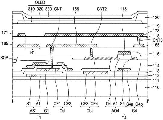
1. A display apparatus comprising:
a substrate including a display area in which a display element is arranged;
a first thin film transistor arranged in the display area and including a first semiconductor layer and a first control electrode;
a first interlayer insulating layer covering the first control electrode;
a node connection line arranged over the first interlayer insulating layer and connected to the first control electrode via a first contact hole;
a first planarization layer covering the node connection line; and
a shielding electrode arranged on the first planarization layer to overlap the node connection line.